
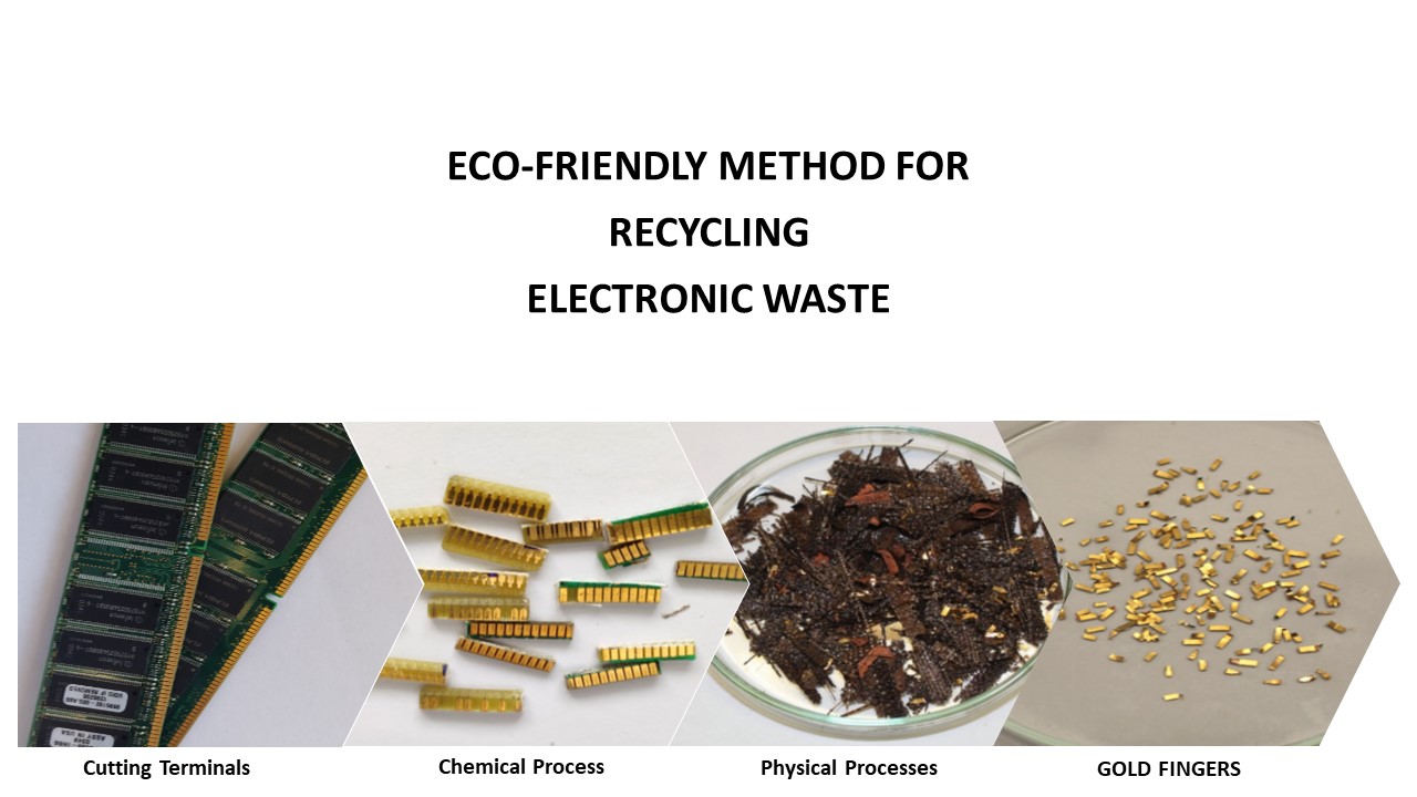
The present invention discloses a new process that combines physical and chemical processes to recover valuable metals, particularly gold, from obsolete printed circuit boards (PCBs) by separating several polymeric laminated layers and copper foils from the gold layers.
Electronic waste (e-waste) is created when an electronic product is discarded after its useful life. The rapid expansion of technology and the consumption-driven society results in a massive amount of e-waste. E-waste is considered the fastest-growing waste stream globally, with millions of tonnes of waste generated every year. Currently, the production of modern electric and electronic equipment requires the use of scarce and expensive resources, as is the case of gold, used to produce new PCBs.
The main innovative aspects of the proposed technology are the minimal generation of wastes, energy consumption and equipment space. Moreover, it is a simple, fast, environmental-friendly and low-cost process that allows the recovery of gold fingers with high yield from the waste’s PCBs. Considering the high price of gold, the isolation of this raw material from obsoletes PCBs is an attractive business opportunity for the recycling companies
Companies handling with manual dismantling of waste electrical and electronic equipm ent.


